


QXS320F28377L is a 32-bit processor benchmarked against TI's TMS320F2837XD series. It is mainly targeted at real-time control applications (e.g., industrial motor drives, photovoltaic inverters and digital power supplies, motor control of electric vehicles, and air-conditioning inverter, etc.).
QXS320F28377LRevB
- Parameters
- Package|Pinout|Dimensions
- Characterization
- Clarification
Main Frequency
300MHz
Kernel Architecture
Dual Core (Computing)
IEEE754 Single-Precision Floating Point Unit (FPU)
Have
Trigonometric Function Gas Pedal(TMU)
Have
Module On Complex Mathematics(VCU-I)
Have
CLA
-
CLB
-
Instruction Storage IRAM
Dual Core Sharing 1MB
Data Storage DRAM
Dual-Core Shared 512KB
Meticulously FLASH
1MB
DMA
6
System Peripherals
-
32-Bit CPU Timer
6
Window Watchdog Timer
2
GPIO
103
AGPIO
21
ADC resolution (bit)
12、14
Number ADC Number
3、5
SamplingG Rate
2.67M、3M
Number Of Channels ADC Input / Ch.
21
CMPSS
7
DAC
12bit
12bit DAC
2
PGA
7
Programmable Gain Amplifier Amplification
3 6 12 24 48
PMBus
1
I2C
1
CAN FD (CAN2.0 Compatible)
2
SPI
2
SCI (uart compatible)
2
LIN (supports switching to uart mode)
1
FSI
1
16bit/32bit EMIF
1
USB2.0
-
EtherCat
-
EPWM Channel
24
HRPWM
16
HHRPWM
16
eCAP
7
HRCAP
2
eQEP
2
SDFM
4
Operating temperature range (°C)
-40℃~125℃
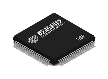
Package Type
LQFP176
Package Size / mm*mm
-
Typology
General Purpose
Availability
Filling
| Type Code | Typology | Number of pins | Length*Width(mm) | Height/Maximum Height(mm) | Pitch(mm) | Spacing | Package Drawing |
|---|---|---|---|---|---|---|---|
| PTPS | HLQFP176 | 176 | 24X24 | 1.4/1.6MAX | 0.5 | Not Uploaded |
QXS320F28377L is a 32-bit processor benchmarked against TI's TMS320F2837XD series. It is mainly targeted at real-time control applications (e.g., industrial motor drives, photovoltaic inverters and digital power supplies, motor control of electric vehicles, and air-conditioning inverter, etc.).
QXS320F28377L has a self-developed 32-bit CPU core benchmarked against the TI C28x, which provides 300MHz of processing power.
QXS320F28377L internal also integrated FPU, TMU and VCU extended instruction set, FPU can provide 32-bit floating-point acceleration instructions, TMU can quickly execute algorithms containing transformations and torque loop calculations of common trigonometric algorithms, VCU extended instruction set to reduce the latency of the coding application of common complex mathematical operations.
The QXS320F28377L utilizes a dual-core architecture, with CPU0 and CPU1 running independently in parallel and communicating with each other. Each core has its own independent storage resources and both have independent access to the major peripherals required in a typical control system. The cores can communicate with each other through interrupts, special registers and shared memory.
The QXS320F28377L also integrates high-performance analog peripherals and enhanced control peripherals. Five independent 12-bit conventional ADCs with a sampling rate of 3MSPS and three independent 14-bit conventional ADCs with a sampling rate of 2.67MSPS manage multiple analog signals accurately and efficiently, ultimately increasing system throughput. Seven PGAs on the analog front-end enable on-chip voltage regulation prior to conversion. Seven analog comparator modules allow continuous monitoring of input voltage levels for trip conditions. Advanced control peripherals (with frequency-independent ePWM/HRPWM and eCAP) provide excellent control of the system. Built-in 4-channel SDFM allows seamless integration of oversampling Σ-Δ modulators on the isolation layer. Connectivity is supported through a variety of industry-common communication ports (e.g., SPI, SCI, I2C, LIN, and CAN2.0, CAN FD), and multiple multiplexing options are provided for excellent signal placement in a wide range of applications. the QXS320F28377L supports both PMBus and FSI. the Embedded Real-Time Analysis and Diagnostics (ERAD) module enables excellent control of the system by providing additional hardware breakpoints and counters for analysis. The Embedded Real-Time Analysis and Diagnostics (ERAD) module enhances the device's debugging and system analysis capabilities by providing additional hardware breakpoints and counters for analysis.
The QXS320F28377L supports up to 512KB of configurable instruction RAM or data RAM, as well as an additional 512KB of instruction RAM and 1MB of Flash memory to accommodate most embedded scenarios.
The QXS320F28377L also supports 8KB of bootloader instruction RAM for flexible configuration of the boot process.
| Typology | Caption | Downloading | Dates |
|---|---|---|---|
| Data Sheet | QXS320F28377LRevB Digital Signal Controller Datasheet | 2025年05月21日 |
- All
- Hardware Development
- Software Development
- Design Tools
- Seal Inside
| Typology | Photograph | Caption | Element | Downloading | Dates |
|---|---|---|---|---|---|
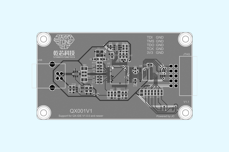
| Development Evaluation Boards |  |
QXS320F280377L Development Evaluation Boards | QXS320F280377L Development Evaluation Boards | 2025年05月28日 |


| Type Code | Typology | Number of pins | Length*Width(mm) | Height/Maximum Height(mm) | Pitch(mm) | Spacing | Package Drawing |
|---|---|---|---|---|---|---|---|
| PTPS | HLQFP176 | 176 | 24X24 | 1.4/1.6MAX | 0.5 | Not Uploaded |
| Typology | Photograph | Caption | Element | Downloading | Dates |
|---|---|---|---|---|---|
| Development Evaluation Boards | |
QXS320F280377L Development Evaluation Boards | QXS320F280377L Development Evaluation Boards | 2025年05月28日 |
| Type Code | Typology | Number of pins | Length*Width(mm) | Height/Maximum Height(mm) | Pitch(mm) | Spacing | Package Drawing |
|---|---|---|---|---|---|---|---|
| PTPS | HLQFP176 | 176 | 24X24 | 1.4/1.6MAX | 0.5 | Not Uploaded |